Micro Via Hole
High-Density Interconnect Solutions
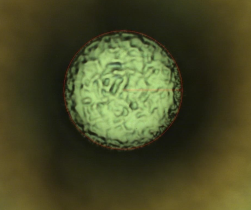
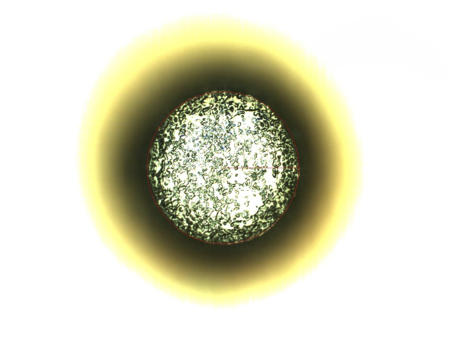
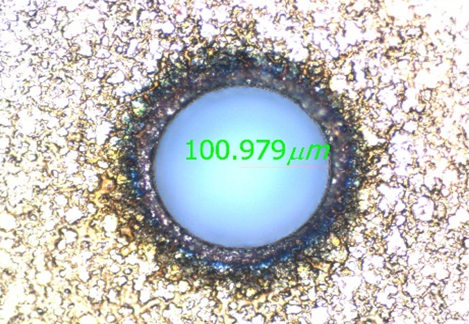
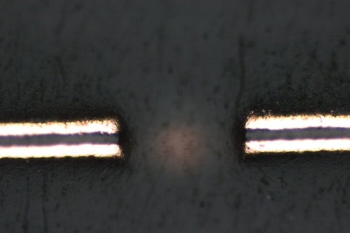
Advanced UV laser micro via hole processing enables the creation of blind vias, skip vias, and through holes with micron-level precision. Our technology supports high-density PCB designs by delivering clean, debris-free vias with perfect registration and depth control.
Key Capabilities
Vision-Driven Alignment
Utilizes 4-point vision registration to compensate for panel distortion and scaling. Ensures precise overlay accuracy by verifying alignment tolerances before processing.
High-Density Interconnects
Seamless processing of UDD, Skip Vias, and Through Holes in a single run, maximizing routing freedom for HDI designs.
Plating-Ready Quality
Delivers smear-free via bottoms for superior plating adhesion, eliminating mechanical stress and ensuring electrical reliability.
Applications & Variations
Explore the full range of capabilities and real-world applications

UDD
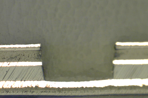
Essential for FPCB interlayer connectivity. Directly processes both copper and insulation layers in a continuous step, eliminating the need for CO2 lasers. Delivers a clean, residue-free copper surface.
Skip Via (Multi-Layer Connection)
An advanced multi-layer interconnect technology that penetrates upper copper layers to reach specific target layers directly. By eliminating the need for sequential stacked vias, it reduces routing congestion and enhances overall structural reliability in HDI designs.
Through Hole (Full Through Drilling)
The standard via method connecting top and bottom layers. Widely used for core processing before lamination and interlayer connectivity in double-sided boards.